





Reading and Writing a BMW EPS Rack over FlexRay

A small on-target agent for the MPC5643L that reads and writes the rack's flash and EEPROM over FlexRay — no JTAG, no opening the case.
Bench notes from the repair side. Everything here was done on removed units on my own test bench, as remanufacturing/diagnostics work, and it all came out of the firmware: the image opened in Ghidra and disassembled, checked against my own dumps and a lot of known-plaintext. I'm leaving the OEM security-access out — it isn't mine to publish, and it isn't in the agent anyway.
TL;DR
The steering ECU across a chunk of the F-series BMW range (internal loader tag 000019EE, "19EE" from here) is built around an NXP MPC5643L — a dual-core lockstep PowerPC running the VLE instruction set — with its calibration split between on-chip C90FL flash and an external M95640 SPI EEPROM. The factory tooling talks to it over FlexRay.
I wanted to read and write both memories on the bench, over FlexRay, without hanging a JTAG probe on every single unit. The route there was a tiny freestanding agent, loaded into the rack's SRAM over FlexRay through an upload path I dug out of the firmware in Ghidra, serving memory operations back to my cable. This post walks the agent: the FlexRay plumbing, the EEPROM and flash drivers, and one protocol trick that fixed a flaky read.
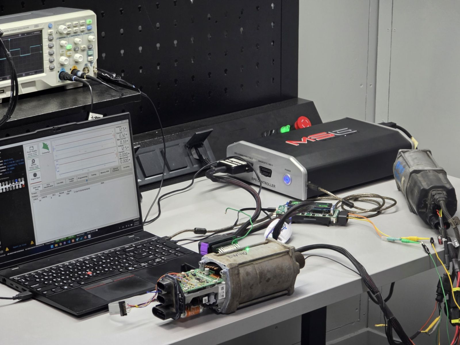
the bench. The MS561 EPS unit (power and diagnostics), the FlexRay cable, a 19EE rack on the ThinkPad running MS561, and the scope up top.
The target
The MPC5643L is a safety-oriented MCU: two e200z4 cores in lockstep, ECC everywhere, and a Freescale/NXP E-Ray FlexRay controller on-die. The numbers that matter for the rest of this post:
| Thing | Where |
|---|---|
| Core | e200z4, PowerPC VLE (variable-length), big-endian |
| Code flash | C90FL controller at 0xC3F88000, flash mapped at base 0x0 |
| "block0" | 0x0000–0x3FFF (16 KB) — calibration + a config CRC-32 |
| EEPROM | external M95640 (64 Kbit SPI) on DSPI_B at 0xFFF94000 |
| FlexRay | NXP E-Ray CC at 0xFFFE0000, message RAM in system SRAM |
One VLE gotcha up front: most stock objdump builds don't decode VLE — a 2005-era binutils gives you garbage. I did the static work in Ghidra with the PowerPC:BE:64:VLE-32addr language. Get the mode wrong and the whole image decodes to nonsense.
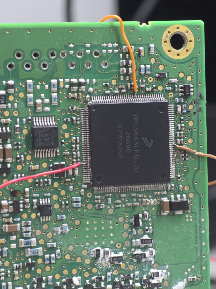
the chip. The rack's main die — SPC5643LFMLQ1, the MPC5643L — with the little 8-pin M95640 SPI EEPROM to its left.
Why an agent, and not "just JTAG everything"
For a long time the only way into this data was brute-force surgery: open the control-unit housing, desolder the EEPROM, read and reprogram it on a cheap external programmer, then solder it back on. It works — plenty of shops still do it — but it's slow and fiddly, and every round trip is another chance to lift a pad or cook the chip. JTAG is tidier, and it's what I used during the reverse-engineering phase, but it still means cracking open that sealed case to reach the debug pads. Neither is something you want to repeat unit after unit on a bench.
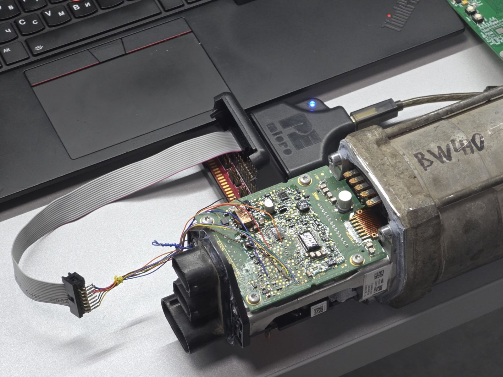
the RE phase. How I read it while reverse-engineering: case open, a P&E probe on the rack's debug header. Fine for the lab — not something you want to do to every unit.
The agent avoids all of it. It rides in over FlexRay — the bus that's already on the connector — so the unit stays shut: no housing to open, no chip to desolder, no pads to lift.
Digging through the firmware in Ghidra, I found the mechanism already there: a path in the loader that pulls a small program into the rack's free SRAM over FlexRay and runs it. So I wrote my own agent for that path, whose job is simply:
poll a FlexRay slot for commands, do the memory operation, answer on another slot.
No libc, no RTOS, no dependencies. It gets its stack pointer and entry from the loader, emits a liveness signature so I can confirm my code is the one running, then sits in a command loop.
Step one: unlocking engineering mode
Before any of this works the rack has to be put into its engineering mode, and that's gated behind UDS security access. The sequence is ordinary UDS:
- DiagnosticSessionControl into the extended session (
10 03), then the engineering session (10 42). - SecurityAccess — the "13/14" level: request the seed (
27 13) and the rack returns an 8-byte seed; compute the response; send the key (27 14). The key is a 4-byte length field followed by a 128-byte signature. - RoutineControl Start (
31 01 03 0C) — this is what arms engineering mode. I pinned the 030C routine in Ghidra; its RoutineControl dispatcher sits at0x635a0.
The one part I keep to myself is the middle step — how that signature is produced, and the key behind it. That stays on my bench. How BMW cooks it? Go ask them. 😉
Step two: getting the agent onto the chip
There's a loader in the firmware that takes a chunk of code into free SRAM over FlexRay and runs it. I pulled it apart in Ghidra:
- A SETUP command (
00 03) puts the loader's receive task (an RTOS task; its dispatcher at0x80000, handler table at0x40009098) into receive mode; the rack answers with an ack (00 08 51). - The frame receiver at
0x8c664copies incoming data into SRAM only if a state gate at0x7e40is armed to0xFE/0xFF. Otherwise every frame is silently dropped. - What arms that gate is the engineering entry itself: the UDS session sets a state byte (
0x7944) to1, RoutineControl030Cruns its handler, and the eng-entry routine at0x81010writes0x7e40 = 0xFEand starts the task.
The catch that cost me time: SETUP is accepted, the ack comes back, but the burst still won't land. A RAM dump of the rack (ICDPPCNEXUS Hotsync, no reset) showed 0x7e40 = 0 — the receive task wasn't armed, so every frame bailed. Sending faster doesn't help; the receiver has to be armed and stay armed by the time the stream arrives, so the order is arm-030C, wait for the FlexRay cluster to come up, then burst. With the gate held, the code lands in SRAM, runs, and the agent announces itself with its liveness frame (00 4C 8A A0 A1 … BF). No JTAG, case shut.
FlexRay, the way the E-Ray sees it
Everything flows through two FlexRay message buffers (MBs): the agent listens on one and answers on another. The E-Ray's message RAM is a header array plus a data region, and a buffer's config lives in registers at ERAY_BASE + 0x100 + idx*8.
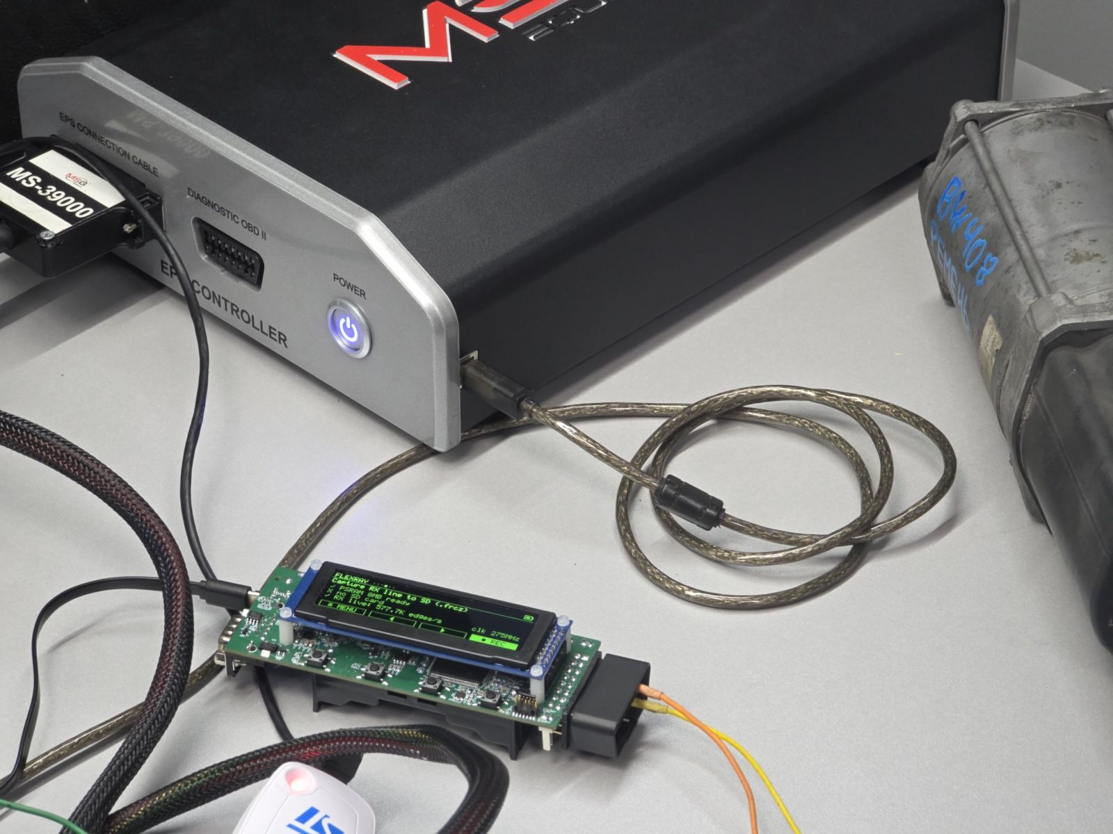
on the wire. The cable sniffing the rack's FlexRay RX line while I worked out the framing — here recording live at ~580K edges/s on a 275 MHz sample clock.
eng_agent.c — E-Ray message-buffer map
#define ERAY_BASE   0xFFFE0000u          /* E-Ray CC; MVR @ +0 reads 0xA268 */
#define FR_MEMBASE  0x40002A00u          /* message RAM base = SYMBADHR:SYMBADLR */

#define MBCCSR(i)  (*(volatile u16 *)(ERAY_BASE + 0x100u + (u32)(i)*8u + 0u))
#define MBCCFR(i)  (*(volatile u16 *)(ERAY_BASE + 0x100u + (u32)(i)*8u + 2u))
#define MBFIDR(i)  (*(volatile u16 *)(ERAY_BASE + 0x100u + (u32)(i)*8u + 4u))
#define MBIDXR(i)  (*(volatile u16 *)(ERAY_BASE + 0x100u + (u32)(i)*8u + 6u))
#define MEM16(off) (*(volatile u16 *)(FR_MEMBASE + (u32)(off)*2u))

/* MBCCSR bits */
#define MB_MTD   0x1000u   /* transmit direction */
#define MB_CMT   0x0800u   /* commit (TX)        */
#define MB_LCKT  0x0200u   /* lock toggle        */
#define MB_DVAL  0x0008u   /* data valid (RX)    */
#define MB_LCKS  0x0002u   /* locked status      */
#define MB_MBIF  0x0001u   /* interrupt flag     */

#define RX_MB 2u           /* I listen on slot 3 (frameID 3 = MB index 2) */
#define TX_MB 0u           /* I answer on  slot 1 (frameID 1 = MB index 0) */
#define KEEP  0xF900u      /* config bits I must preserve on every CSR write */
To touch a buffer you lock it (toggle LCKT, confirm LCKS came back set). The thing that bit me here:
The transmit MB hardware-retransmits its contents every FlexRay cycle. While the controller copies the buffer onto the bus it owns the lock, and a single "toggle and hope" attempt loses the race more often than you'd like.
The naïve single-shot lock returns "didn't get it" silently, the reply never goes out, the far end sees the block go quiet, and the read truncates or crawls while the other side keeps re-asking. The fix is to spin until the controller yields the buffer — there's a free window every cycle. It's safe to retry: a refused LCKT write is simply ignored (status unchanged), so you can't corrupt state, and you stop the instant LCKS reads back set, so you never toggle off a lock you already hold.
mb_lock — spin until the CC yields the buffer
/* Lock a MB. Return 1 if locked, 0 if the CC never yielded it.
   The TX MB retransmits every cycle and the CC owns it while copying out,
   so a single LCKT write often loses the race. Spin until a free window. */
static int mb_lock(u32 i)
{
    u32 spin;
    for (spin = 0; spin < 200000u; spin++) {
        MBCCSR(i) = (u16)((MBCCSR(i) & KEEP) | MB_LCKT);
        if (MBCCSR(i) & MB_LCKS) return 1;
    }
    return 0;
}
static void mb_unlock(u32 i)  { MBCCSR(i) = (u16)((MBCCSR(i) & KEEP) | MB_LCKT); }
static void mb_clrflag(u32 i) { MBCCSR(i) = (u16)((MBCCSR(i) & KEEP) | MB_MBIF); }
Polling a command is then: lock, check DVAL (new frame?), read the header to find where the payload lives and how long it is, copy it out, unlock. Sending a reply is the mirror image.
rx_poll / tx_send — one command in, one reply out
/* Poll the RX slot. On a new frame copy up to maxw words into dst, return #words. */
static int rx_poll(u16 *dst, int maxw)
{
    u16 idx, hdr, dataoff, len, p;
    if (!mb_lock(RX_MB)) return 0;
    if (!(MBCCSR(RX_MB) & MB_DVAL)) { mb_unlock(RX_MB); return 0; }
    mb_clrflag(RX_MB);
    idx     = MBIDXR(RX_MB);
    hdr     = (u16)(idx * 5u);                   /* header = idx*5 halfwords */
    dataoff = (u16)(MEM16(hdr + 3) / 2u);        /* header[3] = data byte offset */
    len     = (u16)(MEM16(hdr + 1) & 0x7Fu);     /* header[1] low 7 bits = words */
    if (len > maxw) len = (u16)maxw;
    for (p = 0; p < len; p++) dst[p] = MEM16(dataoff + p);
    mb_unlock(RX_MB);
    return (int)len;
}

/* Write the response words into the TX slot and commit. */
static void tx_send(const u16 *src, int words)
{
    u16 idx, hdr, dataoff; int p;
    if (!mb_lock(TX_MB)) return;    /* CC busy: skip; the far side re-asks (robust) */
    mb_clrflag(TX_MB);
    idx     = MBIDXR(TX_MB);
    hdr     = (u16)(idx * 5u);
    dataoff = (u16)(MEM16(hdr + 3) / 2u);
    for (p = 0; p < words; p++) MEM16(dataoff + p) = src[p];
    MBCCSR(TX_MB) = (u16)((MBCCSR(TX_MB) & KEEP) | MB_CMT);   /* commit */
    mb_unlock(TX_MB);
    mb_clrflag(TX_MB);
}
The trick that made reads reliable: reply echo
That "retransmits every cycle" behaviour has a second consequence. Because the TX buffer keeps putting its last contents on the bus, the receiver can latch a stale copy of the previous answer — especially the first read after a state change: you end up one request behind, asking for address N and getting the bytes for N-1, and it looks almost right until it very much isn't.
Settle-delays and retries paper over it, but they're a race and they're slow. The deterministic fix is to make every reply self-identifying. The agent stamps two extra words into the frame: an echo token (the address that was requested, or a fixed sentinel for a write) and a reply magic. The cable then refuses any reply whose echo doesn't match the request it just sent. No timing, no guessing — the wrong frame is structurally rejected.
build_response — reply frame + echo stamp
#define REPLY_MAGIC  0x4321u     /* "this is a real data reply" tag */
#define WRPOS_ECHO   0x5A5Au     /* sentinel for the destructive write reply */

/* Build "00 4C 8A <32 data bytes>" from 32 source bytes into the frame buffer. */
static void build_response(u16 *frame, const u8 *data32)
{
    u8 b[36]; int i;
    b[0] = 0x00; b[1] = 0x4C; b[2] = 0x8A;        /* my fixed reply header */
    for (i = 0; i < 32; i++) b[3 + i] = data32[i];
    for (i = 0; i < 62; i++) frame[i] = 0;
    /* pack byte pairs little-end-first into each MB halfword (verified on the bench) */
    for (i = 0; i < 18; i++) frame[i] = (u16)((b[2*i + 1] << 8) | b[2*i]);
}

/* ...and at each call site, right before tx_send: */
frame[18] = (u16)(addr & 0xFFFFu);  /* echo the requested address  */
frame[19] = REPLY_MAGIC;            /* tag it as a fresh data reply */
With the echo in place, full 16 KB reads come back whole every time, instead of truncating partway. If you've fought FlexRay static slots, you know the kind of flaky bug this kills.
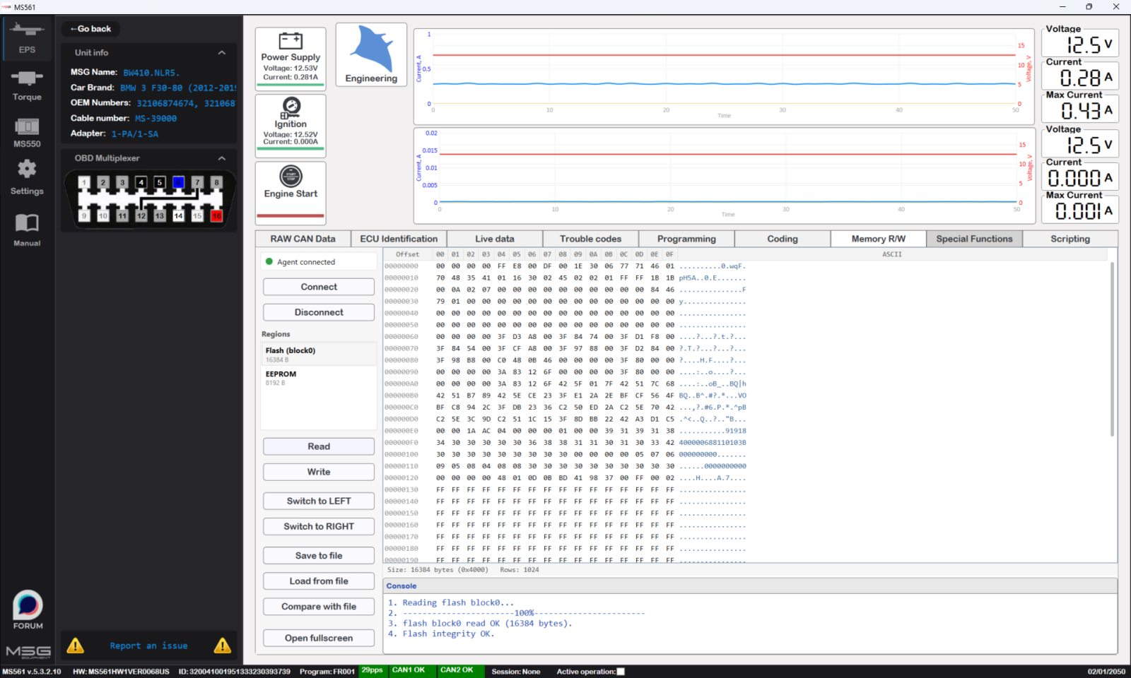
read. A full flash block0 read in MS561: 16 KB back, hex on screen, and the console closing with flash block0 read OK (16384 bytes) and Flash integrity OK. The agent is up (Agent connected) and there's no JTAG on the unit.
Reading the EEPROM — bringing the SPI pins back to life
The M95640 hangs off DSPI_B. The catch: the firmware reads it once at boot and then un-muxes the pads, so by the time the agent runs, those pins aren't SPI anymore. Step one is to put them back — mux CS/SCK/SOUT as outputs and SIN as input through the SIUL pad-control registers, then bring DSPI_B up as a slow, safe 8-bit master. (The pad numbers and CTAR came straight out of the rack's own boot-time EEPROM routine.)
A classic SPI-EEPROM read is opcode 0x03, the 16-bit address, then dummy bytes clocked out to read data back. The only subtlety on this DSPI: chip-select must stay asserted across the whole transaction, so you push command/address/dummy frames back to back with the continue bit set, dropping CS only on the last. One wait-per-byte underruns the FIFO and drops CS mid-transfer. So each data byte is its own tidy 4-frame burst.
spi_ee_read — M95640 burst read on DSPI_B
#define DSPI_B     0xFFF94000u
#define DSPI_MCR   (*(volatile u32 *)(DSPI_B + 0x00u))
#define DSPI_CTAR0 (*(volatile u32 *)(DSPI_B + 0x0Cu))
#define DSPI_SR    (*(volatile u32 *)(DSPI_B + 0x2Cu))
#define DSPI_PUSHR (*(volatile u32 *)(DSPI_B + 0x34u))
#define DSPI_POPR  (*(volatile u32 *)(DSPI_B + 0x38u))

static void spi_ee_init(void)
{
    *(volatile u16 *)0xC3F9004Au = 0x0600u;   /* PCR5  CS0  out */
    *(volatile u16 *)0xC3F9004Cu = 0x0600u;   /* PCR6  SCK  out */
    *(volatile u16 *)0xC3F9004Eu = 0x0600u;   /* PCR7  SOUT out */
    *(volatile u16 *)0xC3F90050u = 0x0100u;   /* PCR8  SIN  in  */
    DSPI_MCR   = 0x80010C00u;   /* master, PCS0 idle-high, flush FIFOs, running */
    DSPI_CTAR0 = 0x38004448u;   /* 8-bit frame, mode0, slow baud (safe) */
}

/* READ (0x03): each byte is a 4-frame burst [cmd, addrHi, addrLo(CONT), dummy].
   The 4th RX byte is the data; CS stays low for the whole burst. */
static void spi_ee_read(u16 addr, u8 *dst, int len)
{
    int i;
    spi_ee_init();
    for (i = 0; i < len; i++) {
        u16 a = (u16)(addr + i);
        volatile u32 to = 0;
        DSPI_MCR   = 0x80010C00u;                      /* flush FIFOs */
        DSPI_SR    = 0xFFFF0000u;                       /* clear status */
        DSPI_PUSHR = 0x80010000u | 0x03u;              /* READ   (CONT) */
        DSPI_PUSHR = 0x80010000u | (u32)(a >> 8);      /* addr hi(CONT) */
        DSPI_PUSHR = 0x80010000u | (u32)(a & 0xFFu);   /* addr lo(CONT) */
        DSPI_PUSHR = 0x00010000u | 0xFFu;              /* dummy, drop CS */
        while (((DSPI_SR >> 4) & 0xFu) < 4u) if (++to > 200000u) break;
        (void)DSPI_POPR; (void)DSPI_POPR; (void)DSPI_POPR;  /* cmd/addr phases */
        dst[i] = (u8)(DSPI_POPR & 0xFFu);                   /* 4th frame = data */
    }
}
Writing the EEPROM — only the bytes that actually changed
Writing the M95640 is the textbook dance: WREN (write-enable, 0x06), then WRITE (0x02) + address + data, then poll the status register's WIP bit until the ~5 ms write cycle finishes. Again, the whole cmd+addr+data rides in one CS-low burst.
spi_ee_write_byte — WREN / WRITE / poll WIP
static void spi_ee_write_byte(u16 addr, u8 val)
{
    volatile u32 to = 0;
    spi_ee_init();
    /* WREN */
    DSPI_SR = 0xFFFF0000u;
    DSPI_PUSHR = 0x00010000u | 0x06u;
    to = 0; while (((DSPI_SR >> 4) & 0xFu) < 1u) if (++to > 200000u) break;
    (void)DSPI_POPR;
    /* WRITE 0x02 + addrHi + addrLo + data (CS held, drop after data) */
    DSPI_MCR = 0x80010C00u; DSPI_SR = 0xFFFF0000u;
    DSPI_PUSHR = 0x80010000u | 0x02u;
    DSPI_PUSHR = 0x80010000u | (u32)(addr >> 8);
    DSPI_PUSHR = 0x80010000u | (u32)(addr & 0xFFu);
    DSPI_PUSHR = 0x00010000u | (u32)val;
    to = 0; while (((DSPI_SR >> 4) & 0xFu) < 4u) if (++to > 200000u) break;
    (void)DSPI_POPR; (void)DSPI_POPR; (void)DSPI_POPR; (void)DSPI_POPR;
    /* poll WIP until the write cycle completes (~5 ms) */
    to = 0; while ((spi_ee_rdsr() & 0x01u) && (++to < 100000u)) { }
}
Two deliberate safety choices in how this gets driven:
- The write command carries a guard byte. A write is honoured only if a fixed guard value is present in the command word. A stray or corrupted frame can't accidentally program the EEPROM — it just gets dropped.
- The host writes a diff, not a blob. On the MS561 side I keep the last full EEPROM read as a snapshot; a write only touches the bytes that differ from it (and never the volatile runtime fields), then reads the window back and verifies it landed. If you've ever bricked a module by rewriting a byte you didn't mean to, you'll get why.
In the shop this is usually the data side of a belt-jump repair. BMW logs it as DTC 0x482452 — "EPS steering angle sensor: belt jump detected" in our decoder — with 0x4822D9 ("…steering angle invalid") as the hardware-side twin, and a belt-jump counter at DID 0xE33C. Despite the name the belt is usually fine; the module's stored data just no longer matches the rack, and flashing or coding won't clear it. Writing the correct EEPROM back is what puts the data right.
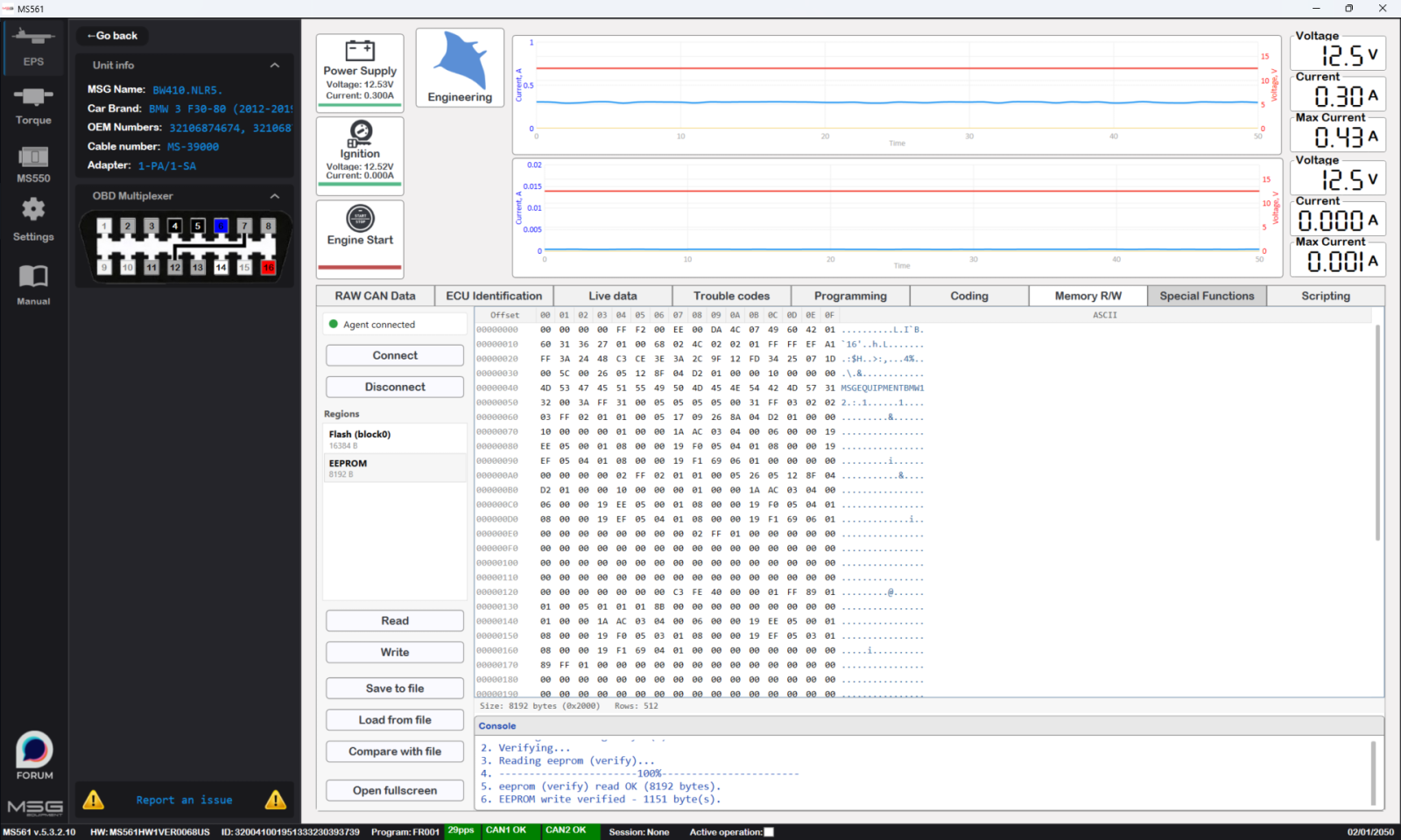
eeprom write. Writing the EEPROM and reading it straight back to check: EEPROM write verified — 1151 byte(s). Only the changed bytes are touched, and the read-back confirms every one.
Writing flash — L/R calibration, with the CRC done on-target
On the 19EE, left- vs right-hand drive isn't cosmetic — on a right-hand-drive rack the assist motor runs the other way, so the flag has to match the car. It comes down to two flag bytes in block0, and block0 is protected by a CRC-32 the firmware checks. Flip the flags without fixing the CRC and the ECU rejects the calibration.
I cracked the recipe on the bench by diffing a genuine LEFT dump against a genuine RIGHT dump:
block0[0xE9]=0x00for LEFT,0x01for RIGHTblock0[0x4E9]=0xFFfor LEFT,0xFEfor RIGHT- a standard zlib/PKZIP CRC-32 (reflected poly
0xEDB88320) overblock0[0 .. 0x3E44), stored big-endian at0x3FCC
Flipping one rack touches exactly those six bytes — nothing else. And it's two flag bytes, not one, because they're a redundant pair: 0x4E9 holds the one's-complement of 0x0E9 (0x00/0xFF, 0x01/0xFE), exactly 0x400 further on, and the top of block0 is mirrored — as a bitwise NOT — at that same +0x400 offset. It's the value-plus-inverse storage safety ECUs use, and both bytes fall inside the CRC-32 region — so a valid edit means setting the pair consistently and recomputing the CRC.
The CRC matched both reference dumps exactly — which is how I knew I had the right span and the right algorithm. So the agent carries its own tiny bit-serial CRC-32 (no table — keeps the agent small) and recomputes the checksum on the rack after editing the flags, so the image it programs is self-consistent.
crc32_zlib — on-target, table-free
/* CRC-32 (zlib/PKZIP: reflected poly 0xEDB88320, init/xorout 0xFFFFFFFF), bit-serial. */
static u32 crc32_zlib(const u8 *p, u32 n)
{
    u32 c = 0xFFFFFFFFu, i; int k;
    for (i = 0; i < n; i++) {
        c ^= p[i];
        for (k = 0; k < 8; k++) c = (c & 1u) ? ((c >> 1) ^ 0xEDB88320u) : (c >> 1);
    }
    return c ^ 0xFFFFFFFFu;
}
Programming itself is the C90FL controller: unlock the block, erase it, then reprogram doubleword by doubleword, skipping blank (0xFF) doublewords. Nothing exotic, but every step is "arm, high-voltage, wait for DONE, check PEG (program/erase good)," and a mistake here is a dead rack, so it's worth being careful and re-locking afterwards.
flash_write_block0 / flash_set_position — erase, program, CRC
#define CFLASH_BASE 0xC3F88000u
#define CF_MCR (*(volatile u32 *)(CFLASH_BASE + 0x00u))
#define CF_LML (*(volatile u32 *)(CFLASH_BASE + 0x04u))
#define CF_SLL (*(volatile u32 *)(CFLASH_BASE + 0x0Cu))
#define CF_LMS (*(volatile u32 *)(CFLASH_BASE + 0x10u))
#define MCR_PGM 0x10u
#define MCR_ERS 0x04u
#define MCR_EHV 0x01u
#define MCR_DONE 0x400u
#define MCR_PEG  0x200u
#define LML_PW 0xA1A11111u
#define SLL_PW 0xC3C33333u

static u8 blk[0x4000];
static int flash_write_block0(void)
{
    int i; volatile u32 to;
    if (!(CF_MCR & MCR_DONE)) return -1;
    CF_LML = LML_PW; CF_LML = 0x001303FEu;     /* unlock block0 */
    CF_SLL = SLL_PW; CF_SLL = 0x001303FEu;
    /* erase block0 */
    CF_MCR = MCR_ERS;
    CF_LMS = 0x00000001u;                      /* select block0 */
    *(volatile u32 *)0x0 = 0xFFFFFFFFu;        /* interlock write */
    CF_MCR = MCR_ERS | MCR_EHV;
    to = 0; while (!(CF_MCR & MCR_DONE)) if (++to > 40000000u) break;
    if (!(CF_MCR & MCR_PEG)) { CF_MCR = MCR_ERS; CF_MCR = 0u; CF_LMS = 0u; return -2; }
    CF_MCR = MCR_ERS; CF_MCR = 0u; CF_LMS = 0u;
    /* reprogram non-blank doublewords from the SRAM snapshot */
    for (i = 0; i < 0x4000; i += 8) {
        u32 w0 = ((u32)blk[i]   << 24) | ((u32)blk[i+1] << 16) | ((u32)blk[i+2] << 8) | blk[i+3];
        u32 w1 = ((u32)blk[i+4] << 24) | ((u32)blk[i+5] << 16) | ((u32)blk[i+6] << 8) | blk[i+7];
        if (w0 == 0xFFFFFFFFu && w1 == 0xFFFFFFFFu) continue;
        CF_MCR = MCR_PGM;
        *(volatile u32 *)(u32)i       = w0;
        *(volatile u32 *)(u32)(i + 4) = w1;
        CF_MCR = MCR_PGM | MCR_EHV;
        to = 0; while (!(CF_MCR & MCR_DONE)) if (++to > 4000000u) break;
        if (!(CF_MCR & MCR_PEG)) { /* re-lock and bail -> restore from backup */ return -3; }
        CF_MCR = MCR_PGM; CF_MCR = 0u;
    }
    CF_LML = LML_PW; CF_LML = 0x001303FFu;     /* re-lock */
    CF_SLL = SLL_PW; CF_SLL = 0x001303FFu;
    return 0;
}

/* snapshot block0, flip L/R flags, recompute CRC, commit */
static int flash_set_position(int right)
{
    int i; u32 crc;
    if (!(CF_MCR & MCR_DONE)) return -1;
    for (i = 0; i < 0x4000; i++) blk[i] = *(const volatile u8 *)(u32)i;
    if (right) { blk[0x0E9] = 0x01u; blk[0x4E9] = 0xFEu; }
    else       { blk[0x0E9] = 0x00u; blk[0x4E9] = 0xFFu; }
    crc = crc32_zlib(blk, 0x3E44u);
    blk[0x3FCC] = (u8)(crc >> 24); blk[0x3FCD] = (u8)(crc >> 16);   /* big-endian */
    blk[0x3FCE] = (u8)(crc >> 8);  blk[0x3FCF] = (u8)(crc);
    return flash_write_block0();
}
A flash erase is the most dangerous thing the agent can do, so the command that triggers it is behind a triple guard — a dedicated opcode, a sentinel byte, and a magic word all have to line up in the same frame before flash_set_position is called. One bad bit anywhere and the request is ignored. The reply carries a distinct echo sentinel (not an address) and the controller's return code in its tail, so the host can tell this frame is the post-write confirmation and read-back-verify the result.
I flipped a test rack LEFT→RIGHT→LEFT, verified the dumps each way, and left it in its original LEFT configuration. ret=0, read-back matches, reversible.
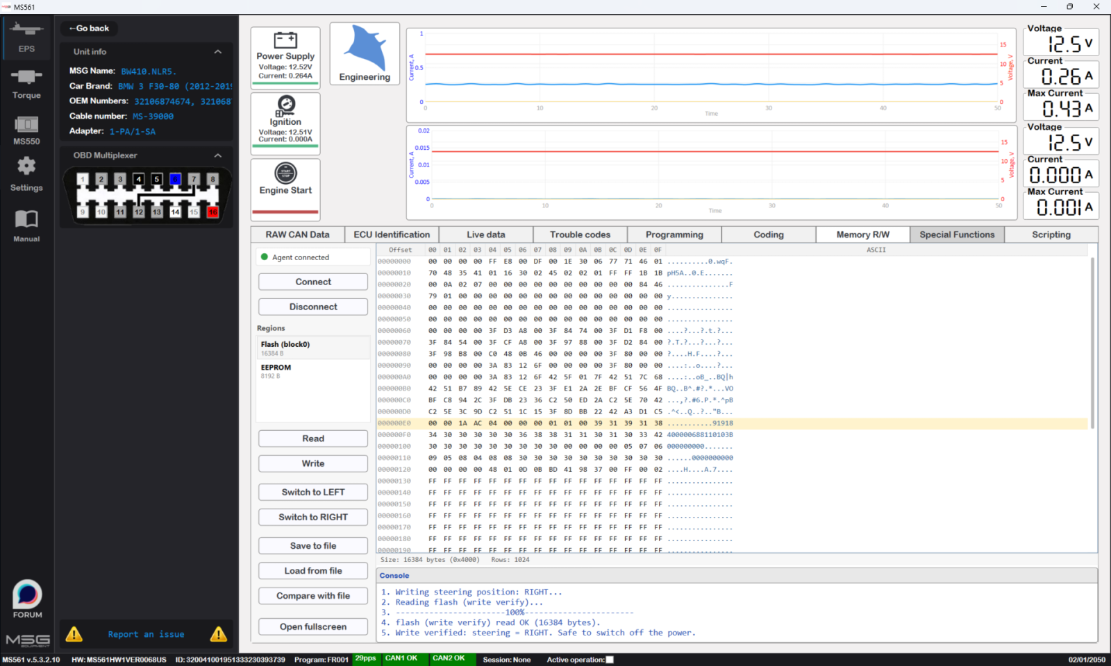
L/R write. The L/R flip on flash, read back to confirm: Write verified: steering = RIGHT. Safe to switch off the power. The changed row is highlighted in the dump, and the CRC was recomputed on the rack.
The command loop, all together
Four commands — read flash, read EEPROM, write EEPROM, write L/R — each answered on the TX slot with the echo stamp. The entry point writes a liveness signature (00 4C 8A A0 A1 A2 … BF) before entering the loop, so I can confirm my code is resident and running purely from the bus, with no JTAG attached.
agent_main — the dispatcher
void agent_main(void)
{
    static u16 frame[64];
    static u8  buf[32];
    u16 cmd[20]; int n, i, ret; u32 addr;

    for (;;) {
        n = rx_poll(cmd, 20);
        if (n < 3) continue;

        if (/* READ flash */ cmd[0] == 0x0017u && (cmd[1] & 0xFF00u) == 0x6300u) {
            addr = ((u32)(cmd[1] & 0xFFu) << 16) | cmd[2];
            for (i = 0; i < 32; i++) buf[i] = *(const volatile u8 *)(addr + i);
            build_response(frame, buf);
            frame[18] = (u16)(addr & 0xFFFFu); frame[19] = REPLY_MAGIC;
            tx_send(frame, 62);
        }
        else if (/* READ eeprom */ cmd[0] == 0x0025u && (cmd[1] & 0xFF00u) == 0x6300u) {
            addr = ((u32)(cmd[1] & 0xFFu) << 16) | cmd[2];
            spi_ee_read((u16)addr, buf, 32);
            build_response(frame, buf);
            frame[18] = (u16)(addr & 0xFFFFu); frame[19] = REPLY_MAGIC;
            tx_send(frame, 62);
        }
        else if (/* WRITE eeprom (guarded) */ cmd[0] == 0x00B7u /* + guard check */) {
            /* ... write the diff bytes, read the window back, reply with read-back ... */
        }
        else if (/* WRITE L/R (triple-guarded, destructive) */ cmd[0] == 0x00B9u /* + guards */) {
            ret = flash_set_position((cmd[1] >> 8) & 0x1);
            for (i = 0; i < 30; i++) buf[i] = *(const volatile u8 *)(u32)i;
            buf[30] = (u8)(ret & 0xFF); buf[31] = (u8)((ret >> 8) & 0xFF);
            build_response(frame, buf);
            frame[18] = 0x5A5Au; frame[19] = REPLY_MAGIC;
            tx_send(frame, 62);
        }
    }
}
The "encryption," briefly — and why I never needed the secret
The memory doesn't come back in the clear; the read path in the firmware XORs it with a keystream. It's often treated as a strong cipher; it isn't. After collecting known-plaintext (erased 0xFF regions, plus the code region that's near-identical between units) the keystream turns out to be a per-address, GF(2)-linear function — an LFSR/CRC of the address, not a real block cipher. There's a statistical tell too: the MSB of each 32-bit keystream word is biased, which is what a cheap linear generator leaks.
Because it's linear, the keystream is fully recoverable from known plaintext: solve a small system over a known block, extend to the rest with one known word per block, and you can decrypt/encrypt any unit without ever extracting a seed or a secret key. So there's no secret to withhold from the agent — it carries none. It hands the raw bytes back and lets the host side do the math. I walked through the security-access sequence earlier; the only piece I hold back is how the key is produced, and that stays in my MS561 software.
I'll describe the shape of the weakness — weak obfuscation should be called weak — but not the per-unit constants or the access handshake. That part isn't mine to hand out.
A note on originality
I've heard the claim that my tools are "1:1 copies" of a certain vendor's, so one note on that.
Everything on this page came out of reverse-engineering the firmware in Ghidra: the register maps, the lock race, the SPI timing, the CRC recipe from my own left/right dumps, the agent source above. The method is here in full, source included.
The protocol itself is my own: the 0x4321 reply echo, the 00 4C 8A reply header, the spin-until-the-CC-yields lock, the triple-guarded erase. If those turn up verbatim in another binary, draw your own conclusion about which way it ran.
Merhaba. Enjoy the read. 👋
Results
| Operation | Transport | Status |
|---|---|---|
| Read flash (16 KB blocks, full image) | FlexRay, no JTAG | diff-0 vs reference, validated repeatedly (~27 s / 16 KB) |
| Read EEPROM (full M95640) | FlexRay, no JTAG | byte-exact, validated (~14 s / 8 KB) |
| Write EEPROM (changed bytes only) | FlexRay, no JTAG | read-back MATCH, reversible |
| Write flash (L/R flags + CRC) | FlexRay, no JTAG | ret=0, read-back verified, reversible |
No JTAG probe on the unit, no secret baked into the agent — just a small program in the rack's SRAM answering questions over FlexRay, and a bench that can now read and write a 19EE rack end to end.
The rest of the agent — the full host-side driver and command set — stays on my bench, but the parts above were the hard ones.
References
- NXP, MPC5643L Microcontroller Reference Manual — Flash Memory Array and Control (C90FL): the LML/SLL lock registers (offsets
0x04/0x0C) and their lock-editing passwords,0xA1A11111and0xC3C33333. - NXP community, C90FL lock-register programming on sibling MPC5xxx parts: MPC5644A example, MPC5744P FLASH block.
Acknowledgements
A special thank you to our colleagues in Latin America & Mexico for their help with the development of this solution. We truly appreciate your support and collaboration!